There are three chief reasons you want to optimize your PCB design for manufacturing.
First, manufacturability. This might seem obvious, but it can be overlooked during the design phase when you’re focused on ensuring all the functionality you want is on the board. You may not consider how your design might present challenges to your Fab House once they have to plan out production. Failure to follow your Fab House’s design rules and capabilities will mean modifying your design very late in the game, causing headaches, and delays, and added expense.
And speaking of cost, that is the second reason to optimize your PCB design for manufacturing. There are a number of variables that will impact the cost of the end product, and it’s important to understand how your design contributes to controlling them (or not).
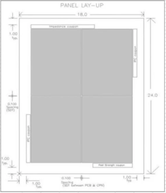
For example, consider your materials utilization. Boards are made in panels. All wasted panel area will end up being scrapped—at your expense! If you understand how your Fab House panelizes, then you can optimize your finished board size to fit a suitable panel and minimize waste.
Likewise, consider the yield from your Fab House. As you push the limits of your Fab House with your design you increase costs. Why? Because your partner’s process is less reliable when they are pushing the edge of their capabilities. Ultimately, to deliver the board you want they must produce extra panels, test them, and scrap the ones that don’t meet quality standards. Again, you’re on the hook for the scraps.
And third, quality. By understanding the manufacturing capabilities of your Fab House and designing with their strengths in mind, you will guarantee your best shot at receiving a quality product with minimal extra costs or waste.
Design Rules to Consider
What are the different PCB design rules that you need to be aware of, and what do they mean? Here are nine that we think are key.
- Panelization and sub-panelization
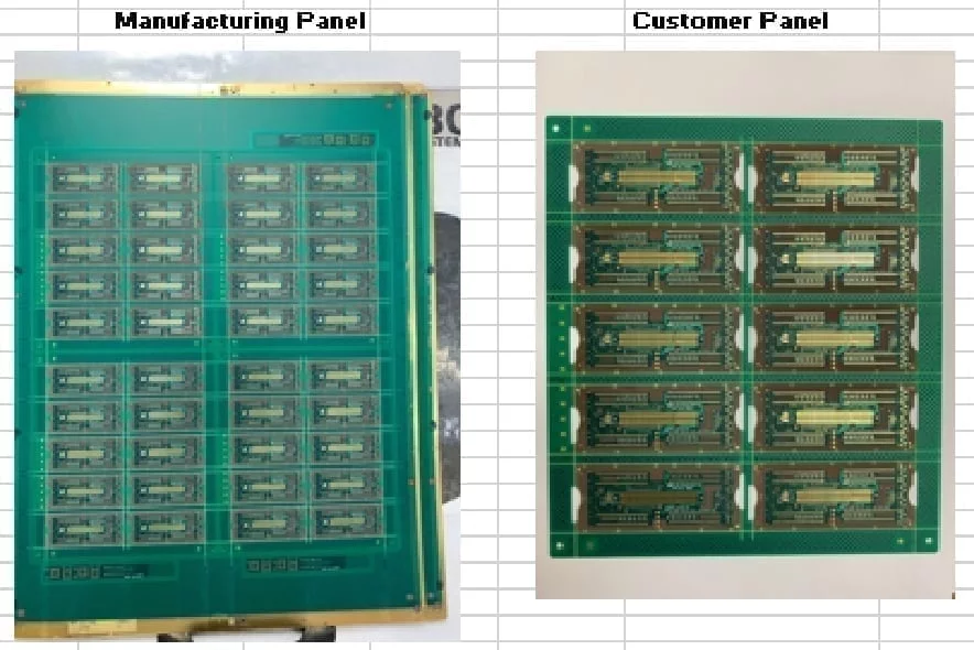
In PCB terminology, “panelization” is a method of designing a number of smaller boards connected together as part of a large, single array that can move through an assembly line easily and then be separated (depanalized) into individual PCBs for packaging or installation. To reap the benefits of panelization consider the overall PCB-array strength (more boards per array is stronger), component layout (connectors near the edges of boards can limit panelization options), PCB shape (if your board isn’t rectangular, alternate images from 90° to 180° to maximize panel space), and location of tooling holes (which can give you space for automated testing if they’re located on edges).
The images below clarify the difference between panelization (“manufacturing panel” - what your Fab House puts through its machines) and sub-panelization (“customer panel” - what your PCB Assembler puts through its machines). Images courtesy of Summit Interconnect.

Also note that typically ½” to 1” or more of the perimeter is lost due to tooling of the Manufacturing panel:

PCBs are made by laminating layers of copper and substrate. Thicker copper increases the current-carrying capacity but increases the PCB cost significantly - so anything thicker than 1oz per square foot is generally reserved for high-power applications. Substrate materials vary widely in their performance - rigidity, thermal performance, and impedance control are some of the common considerations. Match your performance factors with the Fab House’s stock materials and processes to produce the desired result.
Stackup is the arrangement of copper and insulating layers that make up a PCB. More layers can allow you to achieve higher density, increase immunity to external noise and radiation, as well as reduce impedance and crosstalk. Your fabricator can tell you what types of stackups are typical, how the stackup effects cost, and how they should be arranged for reliability and performance.
Traces take up surface area. One of the ways designers manage to fit hundreds or thousands of traces within tight mechanical constraints is to use narrow traces. However, smaller traces are harder to fabricate and can add cost. Work with your Fab House to find the right tradeoff between trace width and cost within their capability.
Clearance refers to the minimum distance between two items on a PCB. For example, trace clearance is the edge-to-edge distance between 2 different traces. A lower clearance allows for higher density, but is harder to fabricate and adds cost.
- Drill sizes and aspect ratio
PCB aspect ratio is the board thickness divided by the diameter of the smallest drilled via. A higher aspect ratio is more difficult to produce, and adds cost. This puts a constraint on the minimum-sized via you can use in your design. An aspect ratio of 10:1 is typically achievable. Higher ratios should be discussed with your Fab House.
- Pad sizes - Annular Rings
Pads are designated surface areas of the PCB that allow for connections to be made by the leads of parts. Annular Rings are the donut-shaped copper areas surrounding plated through-holes or vias. Designers must follow IPC-2221 standards for sizing the annular ring to allow for manufacturing tolerances. This typically means that the radius or the annular ring should be at least 0.5mm to 0.7mm larger than the drill hole diameter.
Uneven distribution of copper (traces and copper fills) in the various layers of a PCB can distort the board, bowing and twisting it. It can also result in uneven plating of copper on your finished product. Most fab houses want to prevent these problems and will either fill the empty area without consulting you, or request that you fix the design yourself. The designer must fill all unused copper area with copper pours AND connect this copper to an appropriate net (GND is typical). As a bonus, the “extra” copper can help distribute heat and may reduce radio-frequency emissions.
IPC standards are the electronics-industry-adopted standards for design, PCB manufacturing, and electronic assembly. There's an IPC standard for every step of PCB design, production, and assembly and you need to ensure your design will be compliant with each. It is crucial that, when designing, you know and understand the IPC class that your PCB will fall under. IPC designates three classes of device:
Class 1 – General Electronic Products: Includes products where the major requirement is the function of the completed assembly.
Class 2 – Dedicated Service Electronic Products: Includes products where continued performance and extended life is required, and for which uninterrupted service is desired but not critical.
Class 3 – High Performance Electronic Products: Includes products where continued performance or performance-on-demand is critical, equipment downtime cannot be tolerated, and end-use environment may be harsh. This equipment must function when required, such as life support systems and other critical systems.
