Are you looking to implement a flex or flex-rigid circuit project? Get in touch with us to access consultation ensuring a first-pass success or as we call it at NeuronicWorks, a board-in-one design.
Designing Flex and Flex-Rigid PCBs
The function of PCB is to connect electronic and mechanical components together using intricate inter-connections. Today there are three main types of PCBs in use: rigid, flexible and flex-rigid circuits. While rigid PCB technology has been around for awhile and is better known, in this blog we will take a look at flex and flex-rigid PCBs, the advantages of using them, the design challenges involved and suggestions on how to best overcome them.
Advantages of flex and flex-rigid PCBs
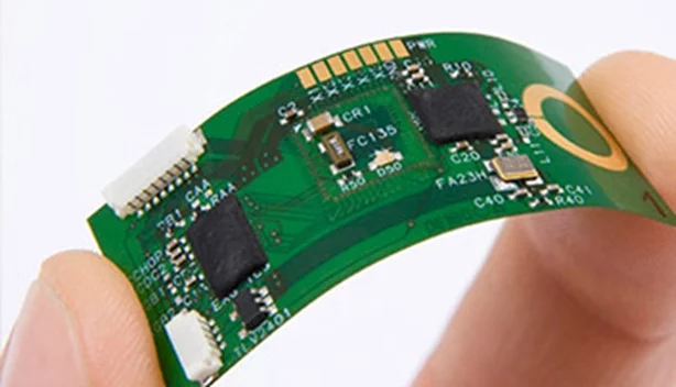
Flexible PCBs, also called flex circuits or flex boards, as the names suggest are ‘flexible’ and can be bent, twisted, folded, or shaped to fit the design’s mechanical constraints. Compared to rigid PCBs, which use fibreglass-reinforced epoxy, flex PCBs use thin non-reinforced plastic sheets (typically made of polyimide) to support circuitry. As a result, they have reduced size, weight, are very thin (can be thinner than 0.1mm) and can curve and bend – making them useful for wearables and other space constrained designs. They are also great for harsh environment applications because polyimide can withstand high temperatures and is resistant to chemical and UV degradation. Flex-PCBs also have excellent shock and vibration performance.
Flexible PCBs are used in applications like consumer electronics, smartphones, automotive electronics, and medical electronics, to name a few.

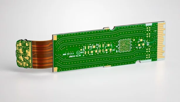
Flex-rigid PCBs have both flexible and rigid areas in one single continuous assembly. The rigid areas support high density circuits, while the flex areas act as cabling between those circuits. No connectors or separate cables are required. Eliminating cables and connectors reduces system size, offers high reliability, and allows for tight impedance control.
Flex-rigid PCBs are widely used in applications like industrial and military applications, aerospace, wearables, and more.

Disadvantages of flex and flex-rigid PCBs
Both Flex and Flex-Rigid boards are pretty expensive as compared to rigid boards.
Flex boards are generally 2 or 3 times the cost of a rigid board, while a flex-rigid board would typically be 3 or 6 times the cost of a normal rigid PCB. The reason for the cost difference is that the raw materials are more expensive and more specialized. The tooling and machining used are different from rigid boards as the flexible boards need to be well supported during manufacturing. There is also a possibility of lower yield while manufacturing, where failed boards would have to be scrapped.
Another point to note is the added complexity when it comes to designing flex and flex-rigid boards. PCB designers will need specialized expertise of flex and flex-rigid design techniques and will have to work closely with the manufacturer at every step to reduce wastage and unnecessary complications.
Integration Challenges
Two key points to keep in mind while designing using flex and flex-rigid boards are manufacturability and reliability. The decisions made during the design process has a lasting impact throughout the manufacturing cycle.
There are different standards to keep in mind while designing for manufacturability. One of the well-known standards is IPC 2223, the Sectional Design Standard for Flexible Printed Boards. It is very important to closely collaborate with the fabrication house or manufacturer for them to abide by the standards best suited for the product. This will help the manufacturer to decide what controls to apply during the manufacturing and inspection process to ensure a seamless process.
The common reliability problems for Flex and Flex-Rigid involve broken copper traces and cracked vias.
Here we will list some of the details of Flex and Flex-Rigid constraints and offer suggestions to overcome them:
1) Avoiding copper breaks – Bend ratio
The first key design rule for reliability is having an adequate bend ratio.
The bend ratio is simply the bend radius (r) divided by the PCB thickness (h). Bend Ratio = r/h. For example, your manufacturer may recommend a bend ratio of 10-to-1. This means the bend radius cannot be less than 10 times the thickness of your PCB. In other words, a 0.1mm thick board should not be bent at a radius less than 1mm. The bend ratio depends on the manufacturing technology and on the intended use (whether it is for a one-time or regular bending): a dynamic flex PCB that bends back and forth during regular use will generally need to have a larger bend ratio than a PCB that is only bent during assembly. For guidelines on bend ratios, consult IPC-2223, and your selected manufacturer.

To maintain flexibility with higher layer counts, it is recommended to stack two-layer flexes using an air-gap technique (discussed in this article). Generally, high layer counts are not recommended in flex designs especially if it is bending repeatedly.
2) Avoiding copper breaks – Perform proper Routing
- It is important to always route traces perpendicular to the bend line. This will ensure elimination of the stress points so that the traces do not break when the flex PCB is bent. In the image below, the bend line is highlighted by the light reflection area and that’s the axis that it is being bend or folded along.

- Avoid abrupt angles while designing and use rounded bends. 45 degree or 90-degree angles, can add stress points when the board bends. Think of this concept as being similar to opening a pop can, when you open the tab of the can, you can bend the tab back and forth a couple of times, before it snaps off. This is because the thin material that connects the tab to the can “host” the stress point.

- Stagger traces to avoid the i-beam effect. Very similar to how in construction, two parallel planes are stacked on a perpendicular line to add strength to a building, in a flex circuit, stacking two traces or more one on top of the other creates an i-beam affect which makes it stronger, but less flexible. It is best recommended to stagger the traces rather than stack them one above the other.
- Use a hatched ground when possible. In rigid PCBs we often use solid grounds for best electrical performance. But using a solid ground on a flex pcb could make it more rigid and more likely to crack and fail. As a compromise between conductivity and flexibility you can use a hatched ground. Unfortunately, hatched grounds are not well-suited to impedance control and high-speed routing. To maintain impedance control, you can selectively route return traces directly under the traces of concern. This is going against the i-beam rule, but it is a better compromise than having a solid ground.

- Avoid stress points. Always transition from wide to narrow traces gradually. Abrupt changes are stress points. In the image below, you can see thin traces going to a connector and you can see an abrupt change point which represents the stress point. The red dotted line in the image represents the weak spot where the traces are likely to break. The suggested method is to use a fillet or a gradual transition from the thin to the thick. When using vias in flex PCBs, use teardrops to connect traces to vias or plated through-holes. This creates a smooth transition, free of stress points.
3) Avoiding Via Cracks
- As much as possible avoid vias in the bend area. Bending a via causes stress and cracks that ultimately cause malfunctions and failures.
- In Flex-rigid boards, in between the flex and rigid portion is the area called the transition zone. This is where the assembly changes from rigid to flex. Flexible substrates continue into the rigid region to form a solid bond as shown in the image. The flex substrates and adhesives will ‘squeeze out’ during lamination and can damage vias. Manufacturers typically recommend keeping vias, plated through holes and special copper features at least 40mils away from the transition zone (50-60mils is recommended).

4) Avoiding Trace Lifting
Copper traces on flex circuits are held in place by the polyimide coverlay. If an area – such as a connector on a flex circuit – is mechanically stressed, the trace may get pulled off, or “lifted” and ultimately fail. One way at increasing the trace’s adhesion is to increase its surface area so that the coverlay has more to grab on to. For plated through-holes or vias, this takes the form of larger annular rings and/or using anchor points. We can also consider applying stiffeners to harden specific areas of a flex circuit to thicken the flex board in specific areas that are susceptible to excessive pressure.
These are just a few of the considerations to keep in mind while designing with flexible PCBs. While Flex and Flex-Rigid boards due to their intrinsic advantage are proving their worth in countless applications across the globe today, they do require careful design consideration and direct collaboration with your design house and manufacturer.


